Playing around with SDRs for more than 14 years now, I learnt a lot. Not on a very professional level, but on a hobbyist niveau.
I went through developing some firmware for the CY7C68013A, a framework for transferring IQ data from SDRs to processing modules, implemented a spectrum analzer UI, demodulators for all kinds of protocols like GSM or POCSAG, etc etc.
But apart from building cables I never was tinkering with the RF path itself. Neither do I have an amateur radio license, nor did I really design RF hardware. The latter is something I wanted to change and finally did.
Recently I built a 405 MHz tuned ground plane antenna for weather balloon tracking using the rdzsonde ESP32 firmware. Later I added a 6 m long copper tape dipole antenna for the other bands. Having some antennas in my attic now, I wanted a comfortable solution to switch between them.
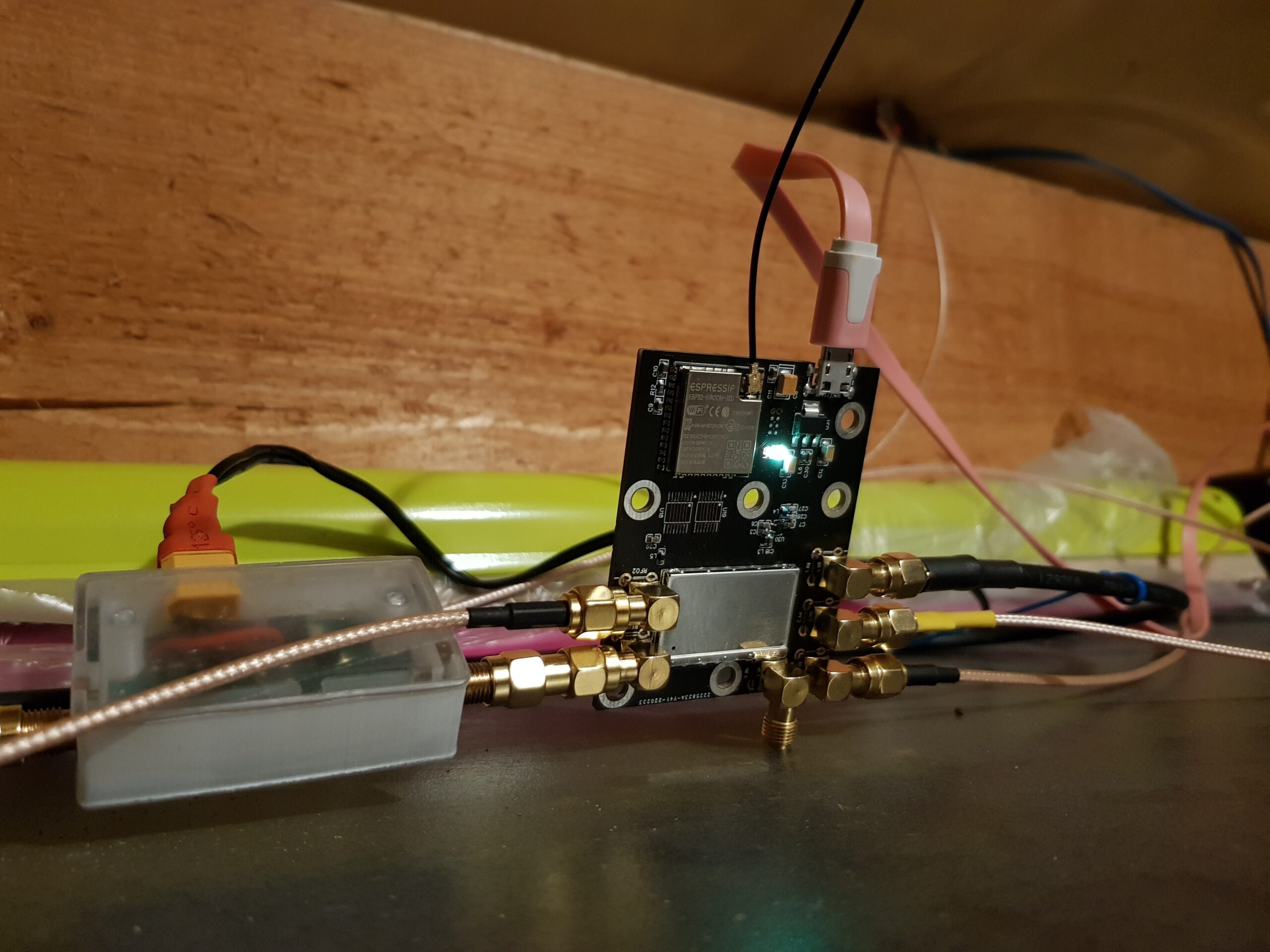
Of course I have choosen an ESP32 for the brain, switching multiple antenna inputs between two outputs. This and a WS2812 for the obligatory RGB colors.
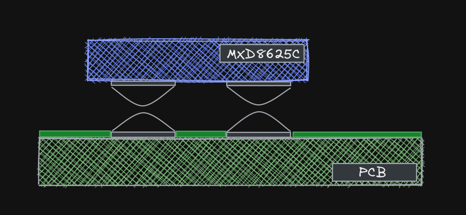
I had the idea to use one MXD8636 SP3T switch per input channel to choose between two RF outputs or a 50 ? termination.
As this switch also has an open position, it is also possible to disconnect the antenna with 25-35 dB isolation. Guess that value is quite okay.
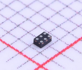
While the switch is quite good with only less than a dB insertion loss, I still placed a switchable 17 dB amplifier using the AD8354. I was not sure if I ever would need this as Tx switcher, so I made the amp completely bypassable using two switches – before and after the amp. The switches I used for that are MXD8625C SPDT in a microscopic 1.1 mm x 0.7mm 6-lead QFN package. Hell is that package small.
Putting all the pieces together, the resulting, simplified schematic view looks like this:
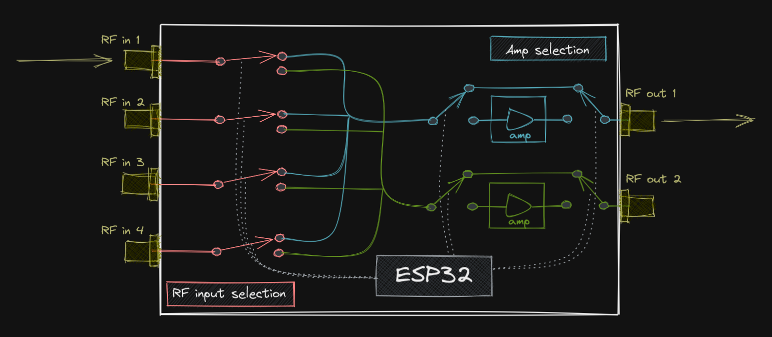
While the RF in are meant as inputs, they are still just connected via the RF switch and thus can also be used to feed a signal to another receiver. Just without any preamp.
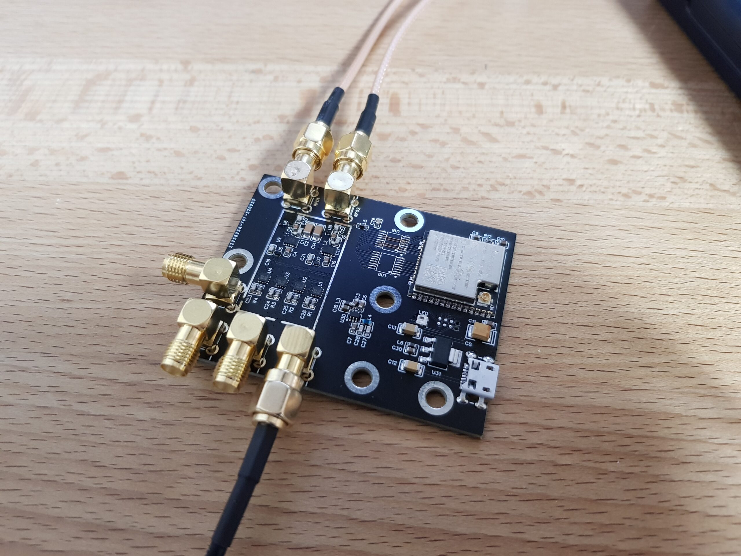
I started the design in february 2022 using EasyEDA and ordered the PCBs at JLCPCB about 10 days later. The parts were picked from LCSC so I had all the packages readily available in EasyEDA without big fuzz. As usual, I’ve chosen a black PCB, 4 layers as all of the last ones I ordered.
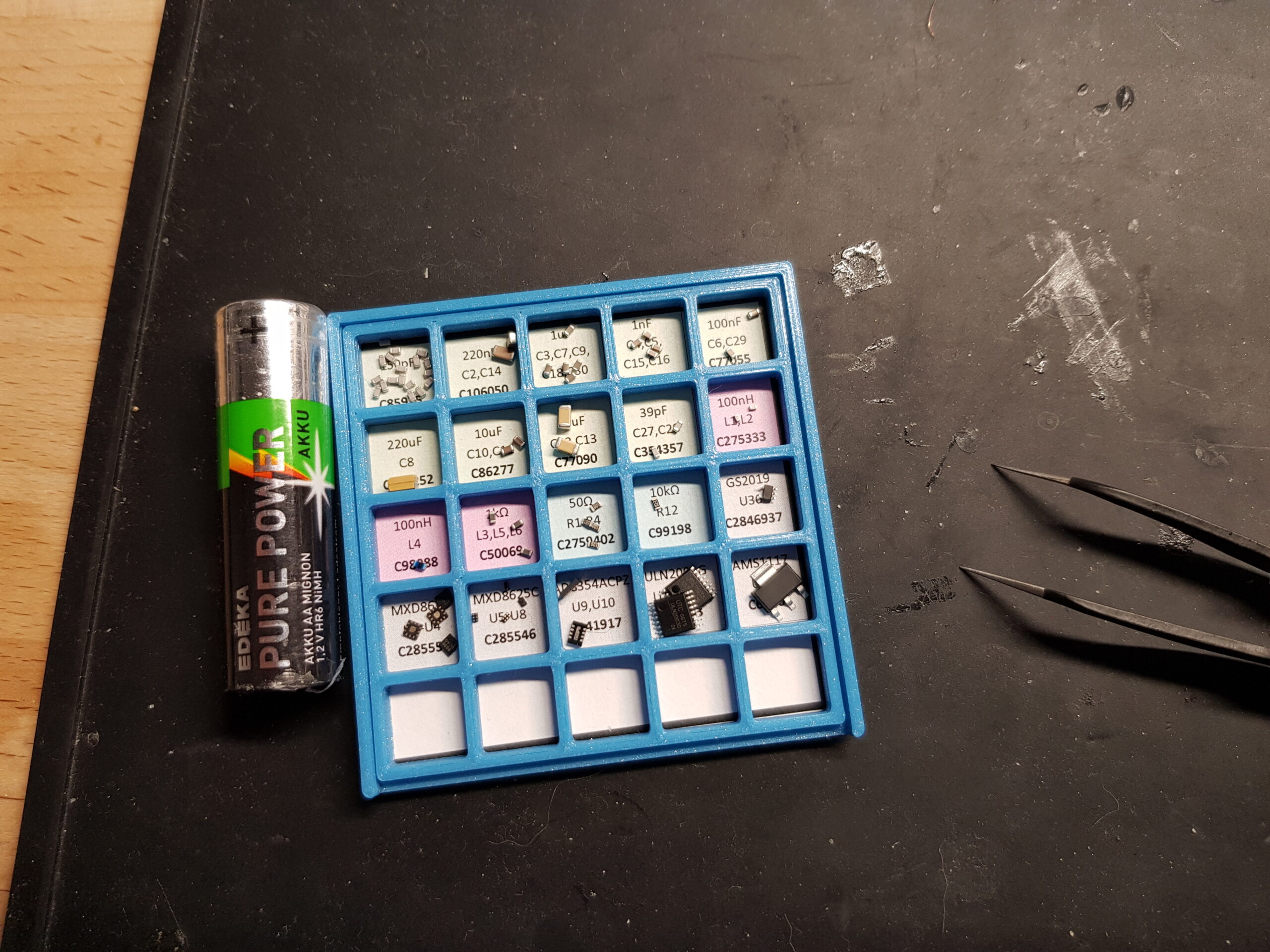
Also like the last ones before, I ordered a stencil, applied solder paste, placed the components and soldered them using a MHP-30 mini hotplate.
I don’t have videos from that process, just from the resulting PCB.
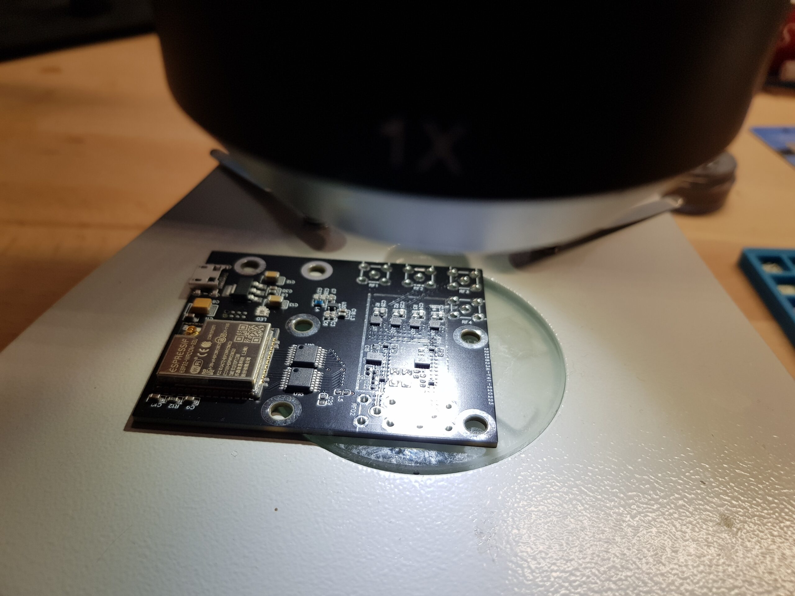
After soldering everything came out quite good except the MXD8625C SPDT. They seemed to have bad contacts due to too few solder underneath. Maybe the holes in the stencil were too small for enough solder to get through.
It took a few tries, but I had to desolder them using the hot plate and then use the soldering iron to put solder onto both the PCB pads of the QFN package as well as the pads of the chip itself. In the end the solder amount per pin was comparable to like a BGA would have.
For soldering I’ve put a small drop of Amtech tacky flux between PCB and SMD component and the surface tension of the solder aligned the part properly. Thats the same mechanism that aligns BGA components perfectly when soldering.
Fixing that for all the switches, the RF path worked perfectly. Luckily no part died during that process.
Then there was just one issue left. I have chosen ULN2003G as level shifters and did not notice that this is just an open collector circuit, so I had to work around that. I just looked at its schematic that shows inverting buffers with protection diodes and didn’t notice that the implementation ist just open collector transistors. Never used those before.
These ULNs were placed to translate from 3.3V to 3.0V for the switches and also meant to have some extra RF decoupling between the ESP32 and the RF path. Removing and bridging them with enamel wire did not fry the switches, so it seems that extra 0.3V is just fine ;)
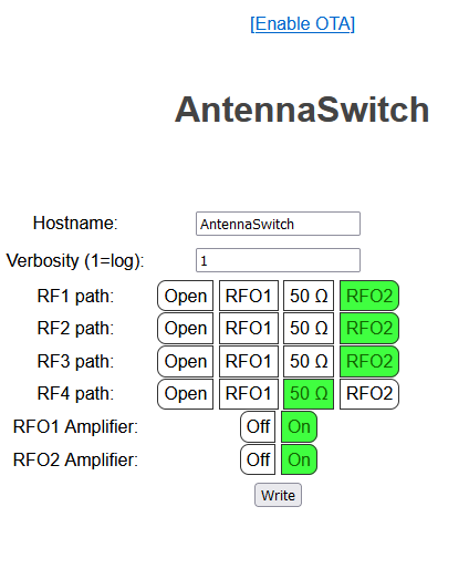
For the software there is nothing special to talk about. Its just a few CSS’ed buttons for selecting which input is fed to which output (RFOx). As the switches are wired in a way that multiple antennas can combined for increasing sensitivity, the RFO2 in the screenshot below gets fed by three antennas. Also the amplifiers can be switched per output path.
One output first feeds into an extra GALI-84+ 25 dB amplifier before going 6 m cable downstairs.
Here you can find more the schematics and the PlatformIO sources
Related Posts
Dyson v15 Battery Notes

ISO15693 Block for AARONIA RTSA-Suite