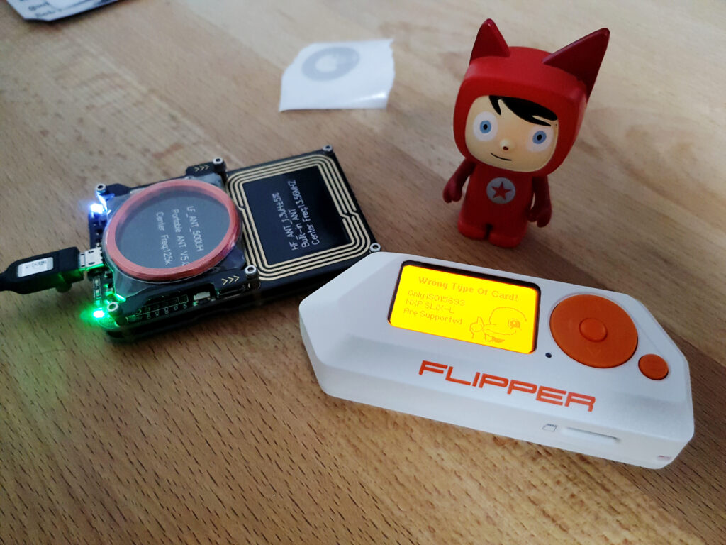
Some time ago, I blogged about my work on Flipper Zero support for Toniebox figurine.
It took a while to get it through, but finally the Flipper Zero Dev team accepted my pull request for the ISO15693 emulation.
Why is this such a big deal?
The NFC chip in use, the ST25R3916, essentially does not have ISO15693 passive target support. In other words, it doesn’t support emulating tags. However, it does have a pass-through mode, which allows the microcontroller (µC) to control load modulation and read field strength. This means the host µC can utilize the NFC chip as an RF front-end, but can modulate any signal, not just the ones the chip inherently supports.
Nevertheless, this requires significant effort, such as synchronizing to the bit periods of the reader, interpreting the modulated signal, and rebuilding the data bits from that signal. Similarly, when sending data, it’s necessary to modulate the carrier load at the right time.
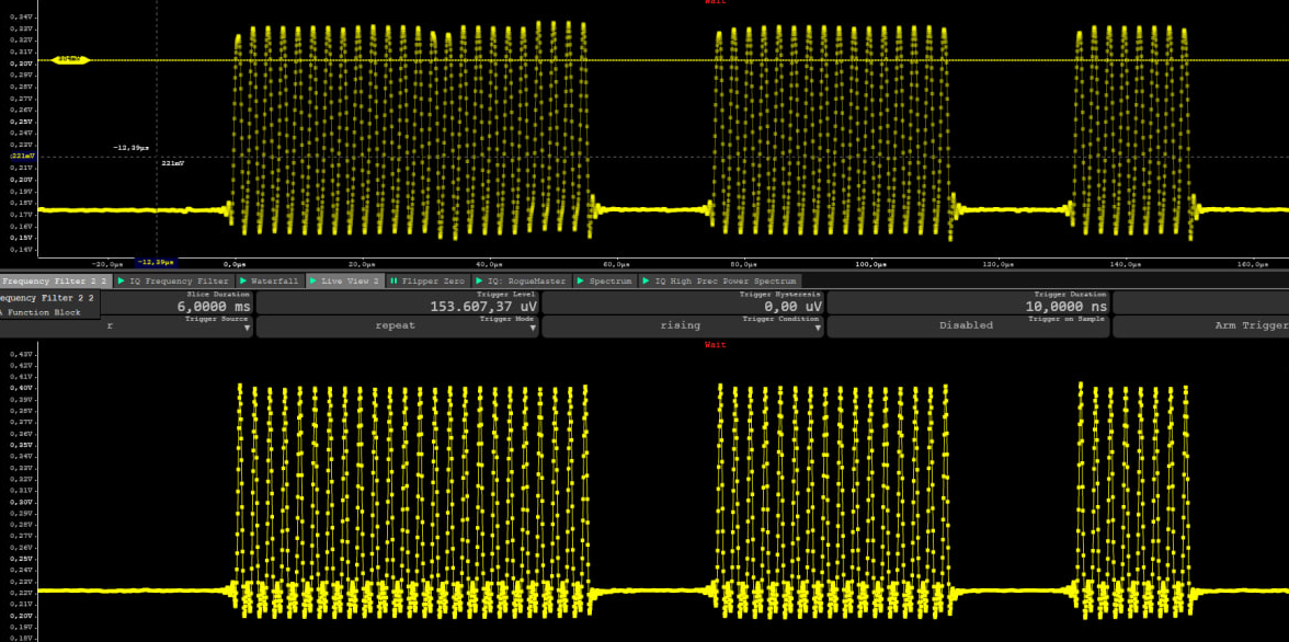
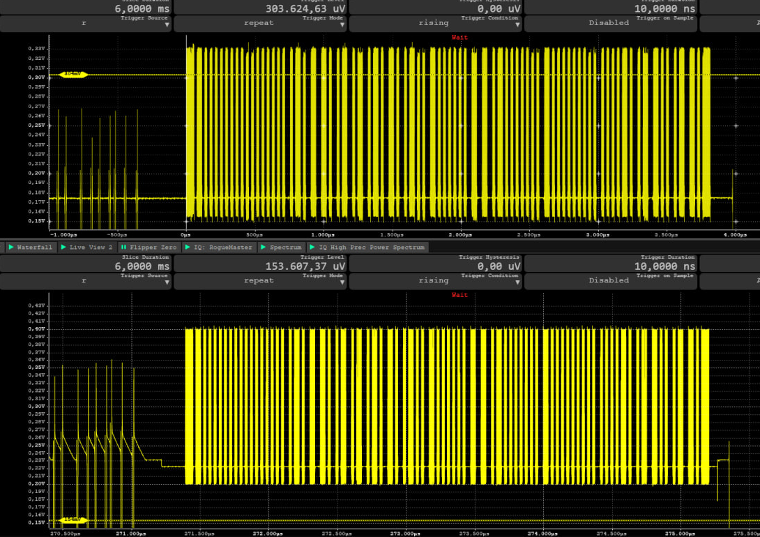
As you can see in the graph, these NFC chips modulate the field by issuing or releasing a load on the NFC coil, causing the field’s strength to go up and down. ISO15693-2 specifies to modulate the field with a overlayed signal of 423 kHz as described in my previous post about the AARONIA RTSA Suite script.
While this is generally not a significant issue, it does come with its share of timing problems and impacts. As always, timing is crucial. Given that you have an embedded operating system that cannot be entirely blocked while sending, using a peripheral timer is the only viable choice.
Precompute timer values?
You certainly can precompute all edges and durations before sending, but memory size will quickly become an issue.
For every single bit you send back to the reader, you need about 17 pulse durations of storage. Depending on how you store the timer values, this could result in more than 4k timer values, thus 16 KiB of memory, that you need to precompute if you want to be able to respond with 32 bytes. While this may not seem too much of memory for the microcontroller (µC) in use, the time needed for precomputing is substantial.
The process of interpreting the request, preparing the answer, and building the response waveform would cause a delay that’s quite long, causing readers to timeout.
Tradeoff approach
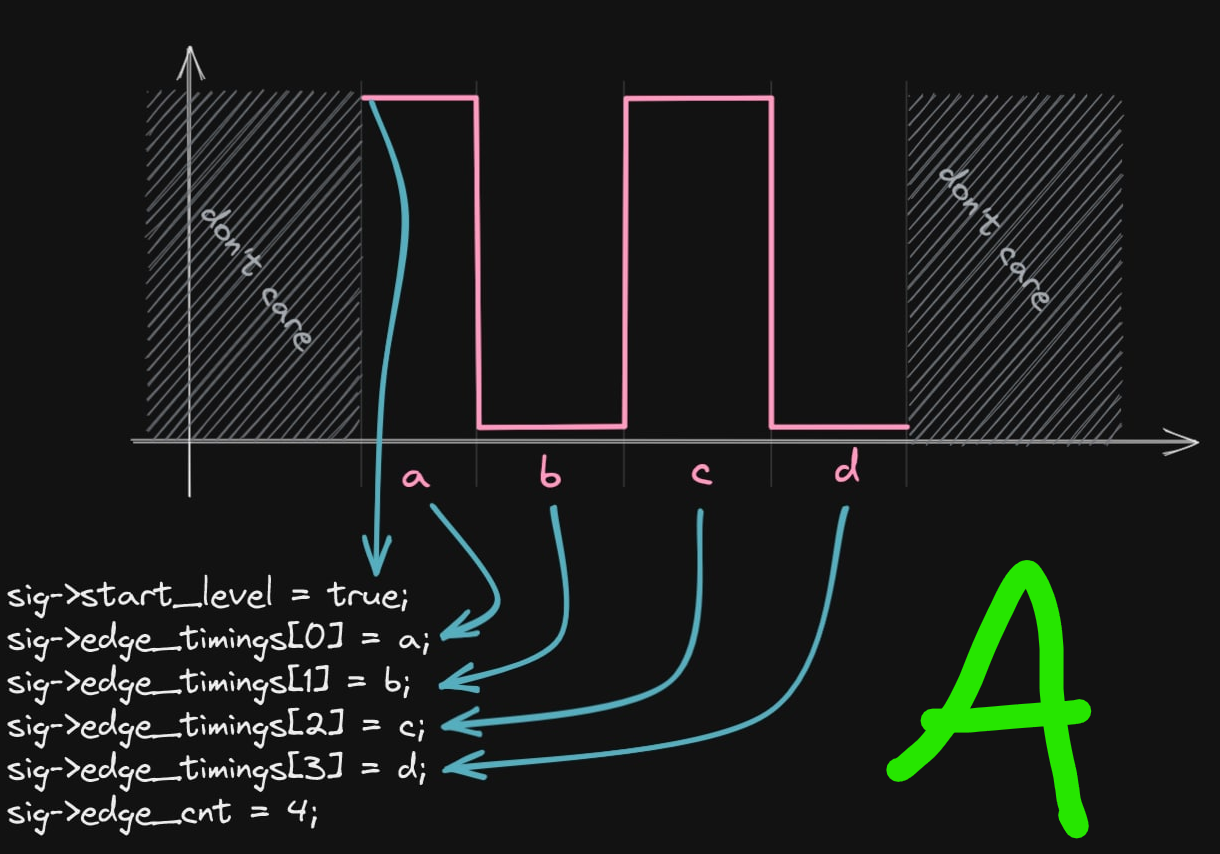
I opted for an optimized approach where the response waveforms (such as “Figure 11 – Logic 1” above) are stored as precomputed basic “signal” blocks, along with other signals like “SOF”, “Logic 0”, and “EOF.” All these signals are then referenced in a so-called “sequence,” which consists only of a list of indices indicating which of the precomputed signals should be sent sequentially.
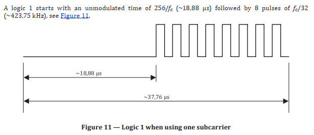
To give a practical example, let’s assume the ID of the SOF (start of frame) is assigned as #0, a logic 0 is #1, a logic 1 is #2, and the EOF (end of frame) is #3, as per the code I implemented. Now, if we need to send a response sequence that reads “SOF, 0, 1, 0, 0, 1, 0, 1, 1, EOF”, the corresponding sequence using these indices would be “0, 1, 2, 1, 1, 2, 1, 2, 2, 3”. If we ignore the basic building blocks, this optimized sequence only occupies 10 bytes, representing a significant reduction from the 1 KiB that would have been used otherwise.
While sending this sequence, the code in digital_sequence_send first fills a buffer of timer values and initiates the DMA -> Timer transactions. As the timer waits for the specified pulse lengths, the DMA loads the next pulse length and anticipates that the main µC will fill the ringbuffer in due time.
So this approach scales better as the basic building blocks are statically occupying memory and every byte to be sent, just causes 8 byte of extra memory usage, instead of 137 timer values.
As a result, we’ve split the process of sending the response into distinct parts, each serving a specific purpose:
– Build a byte-buffer with the response to send.
– Create a sequence of snippets (signals) to send based on the bits in the response buffer.
– Feed those signals into a ringbuffer.
– Keep the DMA and Timer happy, doing the accurate GPIO modulation.
This method allows for the efficient transmission of data, while minimizing the memory footprint and ensuring the accurate timing of signals.
Trial and error
I experimented a lot and tried SEVERAL methods of implementing this stuff. However, the current state proved to be the most efficient, causing the least delay before sending can start, and not causing any jitter due to caching if we modulated the GPIO with software only. Still, there are limitations, and I already have a more optimized version the the queue, as sending 33 bytes, like a SLIX2 would do, was too much for the current state. In the end, I undoubtedly invested more than 100 hours in all this, reinventing the IO routines numerous times, which is a story in itself.
Improvements welcome
I believe there could be better methods to achieve this. If you have found an efficient solution, please feel free to contact me. However, please be aware that you’ll have to manage a mix of 1.18 µs pulses, 18.88 µs delays over a total duration of more than 10 ms.
This was some serious journey
Ultimately, the pull request was merged and the Flipper Zero now supports ISO15693 emulation.
In the words of Skotopes, “this was some serious journey.”

Related Posts
Flipper Zero for Toniebox figurines
An ESP32 based RF antenna matrix